- 您现在的位置:买卖IC网 > Sheet目录3753 > ATMEGA169P-16MCHR (Atmel)MCU AVR 16KB FLASH 16MHZ 64-VQFN
104
8018P–AVR–08/10
ATmega169P
If external pin modes are used for the Timer/Counter0, transitions on the T0 pin will clock the
counter even if the pin is configured as an output. This feature allows software control of the
counting.
14.9.2
TCNT0 – Timer/Counter Register
The Timer/Counter Register gives direct access, both for read and write operations, to the
Timer/Counter unit 8-bit counter. Writing to the TCNT0 Register blocks (removes) the compare
match on the following timer clock. Modifying the counter (TCNT0) while the counter is running,
introduces a risk of missing a compare match between TCNT0 and the OCR0A Register.
14.9.3
OCR0A – Output Compare Register A
The Output Compare Register A contains an 8-bit value that is continuously compared with the
counter value (TCNT0). A match can be used to generate an Output Compare interrupt, or to
generate a waveform output on the OC0A pin.
14.9.4
TIMSK0 – Timer/Counter 0 Interrupt Mask Register
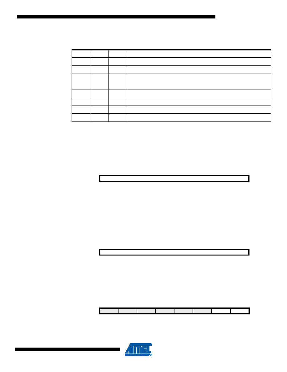
Table 14-6.
Clock Select Bit Description
CS02
CS01
CS00
Description
0
No clock source (Timer/Counter stopped)
001
clkI/O/(No prescaling)
010
clkI/O/8 (From prescaler)
011
clkI/O/64 (From prescaler)
100
clkI/O/256 (From prescaler)
101
clkI/O/1024 (From prescaler)
1
0
External clock source on T0 pin. Clock on falling edge.
1
External clock source on T0 pin. Clock on rising edge.
Bit
765
432
10
0x26 (0x46)
TCNT0[7:0]
TCNT0
Read/Write
R/W
Initial Value
0
Bit
765
432
10
0x27 (0x47)
OCR0A[7:0]
OCR0A
Read/Write
R/W
Initial Value
0
Bit
7654
32
1
0
(0x6E)
–
–OCIE0A
TOIE0
TIMSK0
Read/Write
RRR
R/W
Initial Value
0000
00
0
发布紧急采购,3分钟左右您将得到回复。
相关PDF资料
2-1546217-0
TERM BLK RCPT 20POS SIDE 5.08MM
1-1546217-9
TERM BLK RCPT 19POS SIDE 5.08MM
1-1546217-8
TERM BLK RCPT 18POS SIDE 5.08MM
1-1546217-7
TERM BLK RCPT 17POS SIDE 5.08MM
1-1546217-6
TERM BLK RCPT 16POS SIDE 5.08MM
1-1546217-5
TERM BLK RCPT 15POS SIDE 5.08MM
1-1546217-4
TERM BLK RCPT 14POS SIDE 5.08MM
1-1546217-3
TERM BLK RCPT 13POS SIDE 5.08MM
相关代理商/技术参数
ATMEGA169P-16MCU
功能描述:8位微控制器 -MCU AVR 16KB, 512B EE 16MHz 1KB SRAM, 5V
RoHS:否 制造商:Silicon Labs 核心:8051 处理器系列:C8051F39x 数据总线宽度:8 bit 最大时钟频率:50 MHz 程序存储器大小:16 KB 数据 RAM 大小:1 KB 片上 ADC:Yes 工作电源电压:1.8 V to 3.6 V 工作温度范围:- 40 C to + 105 C 封装 / 箱体:QFN-20 安装风格:SMD/SMT
ATMEGA169P-16MU
功能描述:8位微控制器 -MCU AVR 16K FLASH 512B EE 1K SRAM LCD ADC RoHS:否 制造商:Silicon Labs 核心:8051 处理器系列:C8051F39x 数据总线宽度:8 bit 最大时钟频率:50 MHz 程序存储器大小:16 KB 数据 RAM 大小:1 KB 片上 ADC:Yes 工作电源电压:1.8 V to 3.6 V 工作温度范围:- 40 C to + 105 C 封装 / 箱体:QFN-20 安装风格:SMD/SMT
ATMEGA169P-16MU SL383
制造商:Atmel Corporation 功能描述:MCU 8BIT ATMEGA RISC 16KB FLASH 3.3V/5V 64PIN MLF - Tape and Reel
ATMEGA169P-16MUR
功能描述:8位微控制器 -MCU AVR LCD 16KB FLSH EE 512B 1KB SRAM-16MHZ RoHS:否 制造商:Silicon Labs 核心:8051 处理器系列:C8051F39x 数据总线宽度:8 bit 最大时钟频率:50 MHz 程序存储器大小:16 KB 数据 RAM 大小:1 KB 片上 ADC:Yes 工作电源电压:1.8 V to 3.6 V 工作温度范围:- 40 C to + 105 C 封装 / 箱体:QFN-20 安装风格:SMD/SMT
ATMEGA169P-8AU
制造商:ATMEL 制造商全称:ATMEL Corporation 功能描述:Microcontroller with 16K Bytes In-System Programmable Flash
ATMEGA169P-8MU
制造商:ATMEL 制造商全称:ATMEL Corporation 功能描述:Microcontroller with 16K Bytes In-System Programmable Flash
ATMEGA169PA
制造商:ATMEL 制造商全称:ATMEL Corporation 功能描述:8-bit Microcontroller with 16K Bytes In-System Programmable Flash
ATMEGA169PA_1
制造商:ATMEL 制造商全称:ATMEL Corporation 功能描述:High Endurance Non-volatile Memory segments